Manufacturers needing high-conductivity components often struggle with materials that either lack formability or fail to meet electrical performance standards. While copper alloys like brass offer strength, they sacrifice the pure conductivity required for critical electrical applications. This is where Metal Stamping C1100 (Pure Copper) becomes essential. With 99.9% copper content, C1100 delivers unmatched conductivity and ductility—yet stamping it requires expertise to avoid issues like galling, surface scratches, and oxidation. In this guide, we’ll address these challenges, exploring C1100’s properties, processes, and applications to help you achieve reliable, high-quality results.
Metal Stamping Process for C1100 Copper
Stamping C1100 copper demands techniques tailored to its exceptional softness and ductility:
- Progressive Die Stamping: Ideal for high-volume parts like electrical terminals, this process uses a series of dies to shape C1100 in stages. Include annealing steps every 3–4 stations to counteract minimal work hardening, ensuring the material remains malleable.
- C1100 Blanking/Punching/Bending: Blanking requires sharp, polished dies with 5–7% clearance to avoid burrs. For bending, use wide-radius punches (minimum 1× material thickness) to prevent surface cracking.
- Deep Drawing C1100: Its high ductility allows draw ratios up to 3:1, but slow press speeds (8–12 strokes per minute) and heavy lubrication are critical. This prevents friction-induced heat, which can degrade surface quality.
- Annealing Requirements: Heat C1100 to 400–500°C for 1–2 hours, then air-cool, to restore ductility after intensive forming. This step is less frequent than with harder alloys due to C1100’s low work hardening rate.
Properties & Advantages of C1100 Pure Copper in Stamping
C1100’s appeal lies in its unique combination of properties:
- High Conductivity: 98–100% IACS (International Annealed Copper Standard), the highest among commonly stamped metals. This makes it irreplaceable for electrical components where signal or current loss must be minimized.
- Ductility and Formability: With 45–50% elongation in soft temper (O), C1100 bends, draws, and shapes into complex forms without breaking—outperforming most copper alloys.
- Corrosion Resistance: A natural oxide layer protects against atmospheric corrosion, though it’s less resistant to acids than brass. Suitable for indoor and mild outdoor applications.
- Soft Temper Options: Available in O (annealed, softest) and H1 (lightly cold-worked, slightly stronger). O temper is preferred for intricate stamping, while H1 works for parts needing minor strength.
These properties make 99.9% pure copper benefits clear: uncompromised conductivity paired with exceptional formability.
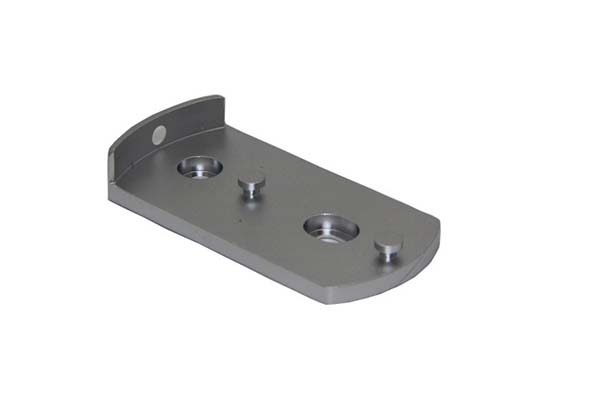
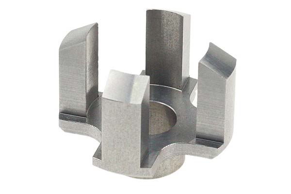
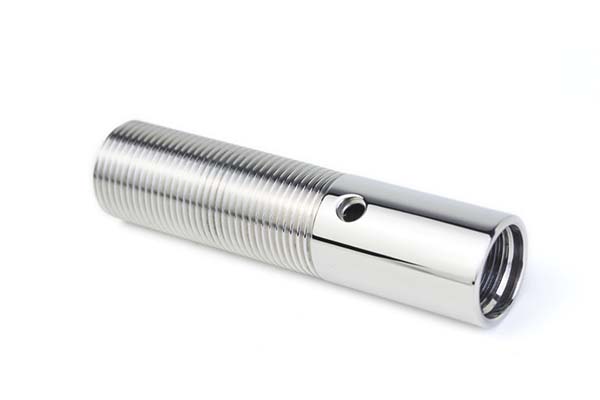
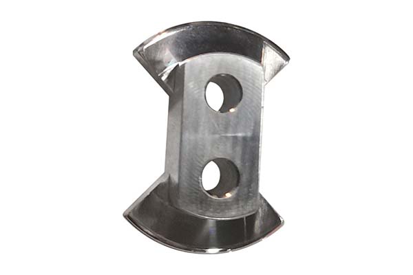
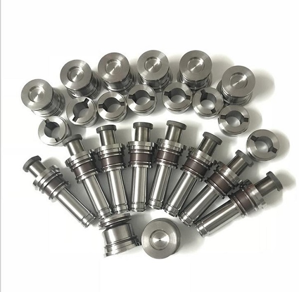
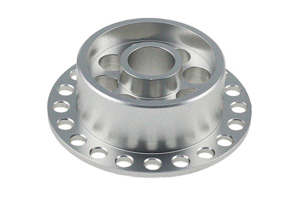
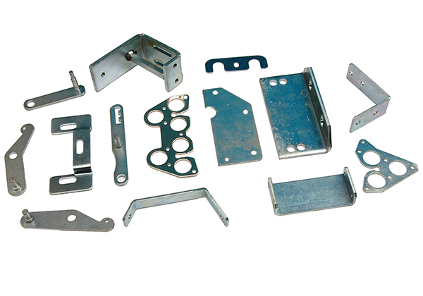
Applications of C1100 Copper Stamped Parts
C1100’s conductivity and formability make it indispensable in:
- Electrical Connectors/Terminals: Ensures low resistance in wiring harnesses, circuit breakers, and battery contacts.
- Heat Exchanger Components: Efficient thermal transfer in radiators and cooling plates for electronics.
- RF Shielding Parts: Blocks electromagnetic interference in smartphones, medical devices, and aerospace equipment.
- Automotive Electrical Systems: Used in sensors, relays, and charging ports where conductivity is critical.
Each application relies on C1100’s ability to deliver both performance and manufacturability.
Design Considerations for Stamping C1100 Copper
Successful C1100 stamping requires careful design choices:
- Minimum Bend Radius: Use 1× material thickness for O temper, 1.5× for H1, to avoid surface cracking. For example, a 0.5mm sheet needs a 0.5mm radius in O temper.
- Grain Direction Effects: Stamp with the grain for maximum ductility in bending; cross-grain stamping may increase the risk of edge cracking.
- Lubrication Requirements: Use non-reactive lubricants (e.g., mineral oils with anti-oxidants) to prevent surface contamination while reducing friction.
- Tolerance Control: C1100’s softness allows tight tolerances (±0.01mm) for critical features, though springback (1–2 degrees) must be accounted for in bending.
Challenges & Solutions in C1100 Copper Stamping
C1100’s softness presents unique hurdles, but solutions exist:
- Galling Prevention Methods: Polish dies to Ra ≤ 0.2μm and use anti-galling lubricants with graphite. Clean dies every 500 strokes to remove copper buildup.
- Edge Cracking Solutions: Deburr blanks before forming and avoid sharp die edges. Anneal after blanking for parts with thin sections.
- Surface Scratch Avoidance: Use plastic interleaving between sheets and handle parts with clean, padded tools. Post-stamping, clean with soft cloths to preserve finish.
- Oxidation Control During Annealing: Anneal in inert gas (nitrogen) environments to prevent discoloration, critical for decorative or high-visibility parts.
Yigu Technology’s Perspective
As a custom manufacturing supplier in China, Yigu Technology specializes in Metal Stamping C1100 (Pure Copper) for electrical and aerospace clients. We use polished carbide dies and inert gas annealing to maintain C1100’s conductivity and surface quality. Our process controls ensure tight tolerances in connectors and shielding parts, leveraging C1100’s formability while preventing galling and scratches.
FAQs
- Can C1100 be stamped into very thin parts?
Yes, down to 0.1mm thickness, but use slow press speeds and light blank holder pressure to avoid wrinkling. O temper is best for thin-gauge work.
- How does C1100 compare to brass for electrical parts?
C1100 offers 3× better conductivity than brass but is softer. Use C1100 for high-performance contacts; brass for parts needing strength over conductivity.
- What post-stamping treatments work for C1100?
Tin plating improves solderability and corrosion resistance. Passivation with citric acid enhances the oxide layer without affecting conductivity.