Manufacturers and designers often face a tough challenge: creating intricate patterns, microscale features, or precise textures on metal, glass, or plastic surfaces without damaging the material or sacrificing accuracy. A medical stent might need 0.1mm-wide channels for drug delivery, a sensor component could require ultra-fine etched lines for conductivity, or a decorative glass panel may demand detailed designs that are both durable and visually striking. Mechanical methods like stamping or machining struggle with such fine details—they can leave burrs, distort thin materials, or fail to replicate complex shapes. This is where surface treatment chemical etching shines. By using controlled chemical reactions to remove material, it creates precise, burr-free patterns with exceptional detail, solving these critical challenges across industries. In this guide, we’ll explore how chemical etching works, its key types, properties, and how it delivers unmatched precision for both functional and decorative applications.
Introduction to Chemical Etching
Chemical etching is a versatile surface treatment that uses chemical reactions to selectively remove material, creating patterns or textures with remarkable precision:
- Definition: Chemical etching is a process where a material (metal, glass, or polymer) is exposed to a chemical solution that dissolves unprotected areas, leaving behind a predefined pattern. The process relies on masking—protecting areas to retain while allowing the etchant to attack exposed surfaces.
- Historical background: The roots of chemical etching date to the 15th century, when artists used acid to etch designs into metal plates for printing. Industrial adoption began in the 19th century for decorative metalwork, and by the 20th century, it became critical for electronics manufacturing. Today, it’s a $3 billion global industry, essential for microfabrication and precision engineering.
- Basic principles: Chemical etching follows four steps: (1) cleaning the substrate to remove contaminants, (2) applying a mask (resist) to protect areas from etching, (3) exposing the substrate to an etchant solution that dissolves unmasked material, and (4) removing the mask and cleaning the surface. The etchant’s strength, temperature, and exposure time control the depth of etching.
- Chemical reactions: Etchants react selectively with the substrate. For example, ferric chloride (FeCl₃) etches copper via Cu + 2FeCl₃ → CuCl₂ + 2FeCl₂, while hydrofluoric acid (HF) etches glass (SiO₂) through SiO₂ + 4HF → SiF₄↑ + 2H₂O. These reactions are exothermic, so temperature control is critical to avoid uneven etching.
- Industrial significance: Chemical etching is vital for producing microcomponents (e.g., semiconductor lead frames with 5μm features), medical devices (stents, surgical tools), and aerospace parts (sensor grids, lightweight panels). It’s preferred for thin materials (0.01-1mm thick) where mechanical processes would cause deformation.
- Environmental considerations: Modern chemical etching prioritizes sustainability. Etchants like ferric chloride are recyclable via filtration systems that remove dissolved metal, reducing waste by 70%. Ventilation systems capture fumes, and neutralization tanks treat wastewater to meet EPA and EU discharge standards, making it cleaner than many traditional machining methods.
- Comparison with other surface treatments: Chemical etching offers unique precision:
| Feature | Chemical Etching | Laser Etching | Mechanical Machining |
| Detail Resolution | 5-50 μm | 10-100 μm | 50-500 μm |
| Burr Formation | None | Minimal | Common (requires deburring) |
| Material Thickness | 0.01-1 mm | 0.01-5 mm | 0.1-100 mm |
| Cost for High Volume | Low (reusable masks) | Medium (no masks) | High (tool wear) |
| Complex Shapes | Excellent (3D coverage) | Good (line-of-sight) | Poor (limited by tool access) |
Types of Chemical Etching
Chemical etching techniques vary by mask type, etchant, and reaction method, each suited to specific materials and applications:
- Wet chemical etching: Uses liquid etchants (e.g., ferric chloride for metals, hydrofluoric acid for glass) in immersion tanks. It’s the most common type, ideal for high-volume production of metal parts (shims, filters) with complex patterns. Wet etching offers uniform material removal and works well with thin substrates.
- Photochemical etching: Combines chemical etching with photolithography. A light-sensitive photoresist is applied to the substrate, exposed to UV light through a pattern mask, and developed to create a precise mask. This method achieves 5-10μm resolution, used for semiconductor components, microfluidic chips, and precision sensors.
- Electrochemical etching: Uses an electric current to accelerate the etching reaction. The substrate acts as an anode in an electrolytic cell, with the etchant as the electrolyte. This method offers faster etching (2-5x speed of wet etching) and better control over depth, used for aerospace parts and tooling with tight tolerances.
- Anodic etching: A type of electrochemical etching where the substrate (typically aluminum) is oxidized to form a porous oxide layer, which is then selectively etched. It’s used to create decorative finishes or porous surfaces for filtration in automotive and industrial applications.
- Selective etching: Targets specific areas using stencils, tapes, or custom masks. It’s ideal for simple patterns (e.g., serial numbers, logos) on metal or plastic parts, offering a cost-effective solution for low-volume runs.
- Isotropic etching: Removes material uniformly in all directions, creating rounded edges. It’s used for applications where sharp corners aren’t critical, such as decorative metal panels or plastic components.
- Anisotropic etching: Etches faster in one direction (e.g., along crystal planes in silicon), creating sharp, vertical walls. This is essential for semiconductor wafers and microelectromechanical systems (MEMS) where precise vertical features are required.
Properties of Chemically Etched Surfaces
Chemically etched surfaces offer a unique combination of precision and performance:
- Detail resolution: Photochemical etching achieves 5-10μm line widths—smaller than a human hair—enabling microscale features like the 10μm channels in medical microfluidic devices. This precision is unmatched by most mechanical processes.
- Surface finish: Chemically etched surfaces are smooth (Ra 0.1-0.5μm) with no burrs, as the etchant dissolves material uniformly rather than cutting it. This is critical for medical devices, where rough surfaces could irritate tissue.
- Dimensional accuracy: Etching depth is controlled within ±1μm, ensuring parts meet tight tolerances (e.g., 0.05mm thick shims with ±0.001mm variation). This precision prevents performance issues in assemblies with tight fits.
- Conformal etching: Chemical etchants reach all exposed surfaces, including recesses, holes, and curved areas, ensuring uniform pattern coverage. This is vital for complex parts like aerospace turbine blades with cooling holes.
- Depth control: Etching depth ranges from 1μm to 1mm, adjustable by varying etchant concentration, temperature, and exposure time. For example, 30°C ferric chloride etches 0.01mm of copper per minute, allowing precise depth tuning.
- Corrosion resistance: Properly cleaned etched surfaces (with all etchant residues removed) resist corrosion as well as unprocessed material. Passivated stainless steel parts etched with nitric acid survive 5000+ hours of salt spray testing (ASTM B117).
- Adhesion: Etched surfaces have micro-textures that improve coating adhesion by 30-50% compared to smooth surfaces. This is used in automotive parts, where paint or plating bonds better to etched substrates.
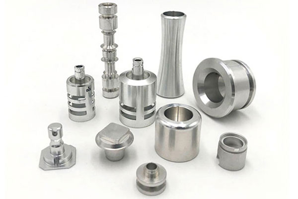
Applications of Chemical Etching
Chemical etching solves diverse challenges across industries, from microelectronics to art:
- Aerospace: Etched sensor grids on aircraft wings measure airflow, while lightweight etched panels reduce fuel consumption. Electrochemical etching creates precise cooling holes (0.5mm diameter) in turbine blades, with ±0.01mm tolerance.
- Medical devices: Photochemical etching produces stainless steel stents with 0.1mm drug-delivery channels, and titanium implants with porous surfaces that promote bone growth. Etched surgical tools have smooth edges to minimize tissue damage.
- Electronics: Semiconductor lead frames with 5μm fine lines are etched using photochemical processes, while flexible circuits use wet etching to create conductive pathways on polymer substrates.
- Consumer goods: Decorative metal panels (smartphone backs, watch cases) use selective etching for logos and patterns. Glassware (drinking glasses, display screens) features etched designs that resist scratching better than printed ones.
- Automotive: Etched shims ensure precise spacing in engine assemblies, while fuel injector nozzles with etched micro-holes (0.1mm) improve fuel atomization and efficiency.
- Jewelry: Precious metals (gold, silver) are etched to create intricate designs, with photochemical etching enabling detailed patterns that rival hand engraving at a fraction of the cost for mass production.
- Filtration: Etched metal filters (stainless steel, nickel) have precise pore sizes (10-100μm) for industrial and medical applications, from water purification to blood filtering.
Chemical Etching Process and Equipment
The chemical etching process and equipment are designed for precision and safety:
- Etching tanks: Made of chemical-resistant materials (polypropylene, PVC) in sizes from 10L (laboratory) to 1000L (industrial). Tanks include heating elements (to maintain 20-60°C) and agitation systems (air spargers or mechanical stirrers) for uniform etchant distribution.
- Chemical solutions: Etchants are tailored to the substrate: ferric chloride (copper, steel), nitric acid (aluminum), hydrofluoric acid (glass), and chromic acid (polymers). Concentrations range from 10-40% to control etching rate.
- Photoresist materials: Liquid or dry films (e.g., diazonaphthoquinone) that harden when exposed to UV light. They’re applied via spraying, dipping, or lamination, with thicknesses from 1-50μm.
- Masks and stencils: Laser-cut polymer stencils (for simple patterns) or photomasks (high-resolution glass plates with chrome patterns) for complex designs. Photomasks are reusable for thousands of parts.
- Temperature control: Digital thermostats maintain etchant temperature within ±1°C, as a 5°C increase can double the etching rate, risking uneven depth.
- Safety equipment: Acid-resistant gloves (nitrile or neoprene), face shields, and fume hoods with HEPA filters. Emergency eyewash stations and neutralizing kits (sodium bicarbonate) are mandatory for handling corrosive etchants.
- Pre-treatment processes: Substrates are cleaned with alkaline degreasers, rinsed, and dried to remove oils and oxides—critical for uniform resist adhesion. Abrasive blasting may be used to improve resist bonding on rough surfaces.
- Post-treatment processes: Etched parts are rinsed in deionized water, then dipped in neutralizing solutions (e.g., ammonia for acid etchants) to stop etching. The resist is stripped with solvents or caustic solutions, and parts are dried in ovens (60-80°C).
Quality Control and Maintenance in Chemical Etching
Rigorous protocols ensure etched parts meet design specifications:
- Dimensional inspection: Optical comparators and coordinate measuring machines (CMM) verify pattern dimensions, with tolerances as tight as ±5μm for semiconductor components. For microscale features, scanning electron microscopy (SEM) checks line width and spacing.
- Depth measurement: Stylus profilometers and laser confocal microscopes measure etching depth, ensuring consistency (±1μm) across batches. This is critical for parts like gaskets, where thickness variation affects sealing.
- Surface inspection: Visual checks under 50-100x magnification identify defects like undercutting (excessive etching under the mask), pinholes, or incomplete etching. Automated vision systems inspect high-volume parts at 1000+ units/hour.
- Etchant analysis: Regular testing (titration, conductivity) ensures etchant concentration stays within 5% of target, preventing slow or uneven etching. Spent etchant is recycled or disposed of per hazardous waste regulations.
- Equipment maintenance: Etching tanks are cleaned weekly to remove sludge, and heating elements are calibrated monthly. Mask alignment systems are checked for accuracy to prevent pattern distortion.
- Safety audits: Monthly inspections of fume hoods, PPE, and emergency equipment ensure compliance with OSHA and EU safety standards. Operators receive annual training on chemical handling and spill response.
- Quality standards: Compliance with ISO 9001 (general manufacturing), ISO 13485 (medical devices), and ASTM B809 (chemical etching of metals) ensures reliability. Aerospace parts meet AS9100 for traceability and performance.
Yigu Technology’s Perspective
As a leading custom manufacturing supplier in China, Yigu Technology specializes in chemical etching for aerospace, medical, and electronics industries. Our capabilities include photochemical etching (5μm resolution), wet etching (metals, glass), and electrochemical etching, handling materials from stainless steel and aluminum to silicon and glass. We use automated etching lines with real-time process monitoring, ensuring depth uniformity (±1μm) and defect rates <0.1%. Our eco-friendly processes recycle etchants and treat wastewater, complying with ISO 14001. With a quality lab featuring SEM and profilometers, we deliver precision parts—from microfluidic chips to aerospace filters—on time and within budget, tailored to client specifications.
FAQs
- What materials can be chemically etched?
Chemical etching works on most metals (copper, steel, aluminum, titanium), glass, silicon, and some polymers (polyimide, PEEK). Each material requires a specific etchant: ferric chloride for metals, hydrofluoric acid for glass, and oxygen plasma for polymers.
- How long does the chemical etching process take?
Etching time depends on depth and material—0.01mm of copper takes ~1 minute with ferric chloride, while 0.1mm of stainless steel takes ~10 minutes. Photochemical etching adds mask preparation time (1-2 days) for new designs, but masks are reusable for high-volume runs.
- Is chemical etching cost-effective for small production runs?
For small runs (<1000 parts), chemical etching is cost-effective if using simple stencils. Photochemical etching has higher initial mask costs but becomes economical for medium-to-large runs (>5000 parts) due to reusable masks and fast processing.