Industries ranging from aerospace to semiconductors demand coatings that can withstand extreme conditions—temperatures exceeding 1000°C, corrosive chemicals, or the need for atomic-level precision. A turbine blade might erode under high-temperature gas flow, a semiconductor wafer could fail due to uneven film layers, or a medical implant might corrode in the body. Physical coating methods like painting or plating can’t meet these demands—they lack the uniformity, purity, or heat resistance required. What’s needed is a process that can create dense, conformal coatings with tailored chemical properties. This is where surface treatment Chemical Vapor Deposition (CVD) delivers. By using chemical reactions to grow films atom by atom, CVD produces coatings that adhere strongly, cover complex shapes evenly, and perform reliably in harsh environments—solving these critical challenges with unmatched precision. In this guide, we’ll explore how CVD works, its key types, properties, and how it transforms surfaces across high-tech industries.
Introduction to Chemical Vapor Deposition (CVD)
Chemical Vapor Deposition (CVD) is a versatile coating process that uses gas-phase chemical reactions to form thin, high-performance films on substrates:
- Definition: CVD is a technique where volatile precursor gases react (or decompose) on a heated substrate surface, forming a solid film. The process occurs in a controlled reactor, with byproducts removed as gases. Films range from 10 nm to 100 μm thick, with composition tailored by selecting precursors.
- Historical background: CVD’s origins date to the 19th century, with early uses in producing lamp filaments. It gained prominence in the 1960s with the rise of semiconductors, where it became essential for depositing ultra-thin, uniform films. Today, CVD is a $20 billion industry, critical for electronics, energy, and advanced manufacturing.
- Basic principles: CVD follows four steps: (1) precursor gases are introduced into the reactor, (2) gases diffuse to the substrate surface, (3) chemical reactions (decomposition, oxidation, or reduction) occur on the surface, forming a solid film, and (4) gaseous byproducts are removed. Temperature (100-1500°C) and pressure drive reactions, ensuring film growth.
- Chemical reactions: Reactions vary by film type. For example, silicon dioxide (SiO₂) forms via SiH₄ + O₂ → SiO₂ + 2H₂, while titanium nitride (TiN) uses TiCl₄ + N₂ + 2H₂ → TiN + 4HCl. These reactions are carefully controlled to ensure purity and uniformity.
- Industrial significance: CVD enables the production of 90% of semiconductor films, from silicon to high-k dielectrics. It’s also vital for aerospace (thermal barrier coatings), energy (fuel cell membranes), and tooling (wear-resistant carbides). CVD coatings extend component life by 5-10x in extreme environments.
- Environmental considerations: Modern CVD uses low-toxicity precursors (e.g., organometallics instead of toxic chlorides) and recovers unreacted gases for reuse. Waste gases are treated (scrubbed or incinerated) to meet emissions standards, making CVD cleaner than many plating processes.
- Comparison with other surface treatments: CVD offers unique advantages for complex coatings:
| Feature | CVD | PVD | Electroplating |
| Conformality | Excellent (covers 3D shapes) | Good (line-of-sight) | Poor (thick at edges) |
| Film Thickness Range | 10 nm - 100 μm | 0.1 - 10 μm | 1 - 20 μm |
| High-Temp Performance | Excellent (up to 1500°C) | Good (up to 800°C) | Poor (melts/degrades) |
| Material Versatility | Metals, ceramics, polymers | Metals, ceramics | Metals only |
Types of CVD
CVD techniques are classified by operating conditions and reaction drivers, each suited to specific applications:
- Thermal CVD: Relies on high temperatures (600-1500°C) to drive reactions, no plasma or catalysts needed. It produces dense, high-purity films (e.g., silicon carbide, SiC) for aerospace and tooling. Thermal CVD is cost-effective for large substrates but unsuitable for heat-sensitive materials.
- Plasma-Enhanced CVD (PECVD): Uses plasma (ionized gas) to activate reactions, reducing temperature requirements (100-400°C). Ideal for heat-sensitive substrates like polymers, glass, and electronics. PECVD deposits dielectrics (SiO₂, SiN) in semiconductors and anti-reflective coatings on displays.
- Low-Pressure CVD (LPCVD): Operates at reduced pressure (0.1-10 Torr), improving gas diffusion and film uniformity. Used for depositing conformal films on complex semiconductor structures (e.g., trenches, vias) where uniformity is critical.
- Atmospheric Pressure CVD (APCVD): Runs at ambient pressure, simpler and faster than LPCVD. Used for large-area coatings like glass (solar panel anti-reflective layers) and architectural films, where high throughput matters more than nanoscale precision.
- Atomic Layer Deposition (ALD): A specialized CVD where precursors are introduced sequentially, reacting one monolayer at a time (0.1-0.3 nm per cycle). ALD achieves atomic-level thickness control (±0.1 nm) and perfect conformality, essential for nanotechnology and fuel cells.
- Metal-Organic CVD (MOCVD): Uses metal-organic precursors (e.g., trimethylgallium) to deposit compound semiconductors (gallium nitride, GaN) for LEDs, lasers, and power electronics. MOCVD enables precise control of film composition.
- Hybrid CVD: Combines techniques (e.g., PECVD + ALD) to balance speed and precision. For example, hybrid CVD deposits a thick base layer via PECVD, then a thin, uniform ALD layer for barrier properties in electronics.
Properties of CVD Coated Surfaces
CVD coatings are engineered to deliver exceptional performance in demanding applications:
- High hardness: Ceramic CVD films (tungsten carbide, WC; silicon carbide, SiC) reach 2000-4000 HV, making them ideal for cutting tools and wear parts. These coatings resist deformation even under high loads.
- Thermal resistance: CVD coatings like hafnium carbide (HfC) and zirconium carbide (ZrC) withstand temperatures up to 3000°C, protecting rocket nozzles and turbine blades in extreme heat.
- Corrosion resistance: CVD diamond-like carbon (DLC) and silicon nitride (Si₃N₄) films act as impermeable barriers, resisting acids, alkalis, and saltwater. Marine components with CVD coatings survive 10,000+ hours of salt spray testing (ASTM B117).
- Conformal coating: CVD uniformly covers complex shapes—deep trenches, sharp edges, and porous structures—with thickness variation <5%. This is critical for semiconductor vias and medical implants with intricate geometries.
- Chemical resistance: CVD films like aluminum oxide (Al₂O₃) resist attack by corrosive gases (e.g., chlorine, sulfur dioxide) and solvents, making them suitable for chemical processing equipment.
- Adhesion: Films grow directly on the substrate via chemical bonding (covalent or ionic), achieving adhesion strengths >50 N/cm². This prevents peeling even under thermal cycling or mechanical stress.
- Dimensional accuracy: Thin CVD films (10 nm-1 μm) preserve tight tolerances (±0.001 mm), essential for precision parts like sensor components and microelectromechanical systems (MEMS).
Applications of CVD
CVD coatings enable innovation in industries requiring high-performance surfaces:
- Semiconductors: CVD deposits nearly all films in integrated circuits—silicon (epitaxy), dielectrics (SiO₂, Si₃N₄), and metals (tungsten). ALD, a CVD variant, creates ultra-thin (1-5 nm) barrier layers for advanced chips (5 nm and smaller).
- Aerospace: Thermal barrier coatings (yttria-stabilized zirconia, YSZ) via CVD protect turbine blades from 1200°C+ gas temperatures, improving engine efficiency by 5-10%. CVD SiC coatings on rocket nozzles withstand re-entry heat.
- Energy: CVD deposits fuel cell membranes (proton-exchange layers) and solar cell anti-reflective coatings, increasing energy conversion efficiency by 10-15%. Wind turbine bearings use CVD WC coatings to reduce wear.
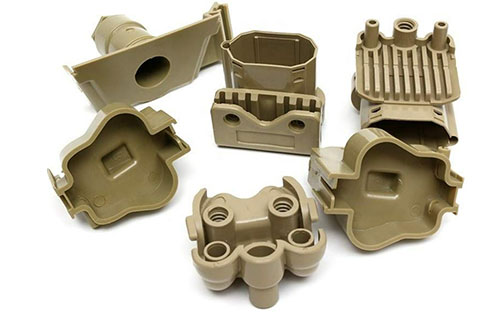
- Tooling: Tungsten carbide (WC) and titanium carbide (TiC) CVD coatings on cutting tools enable machining of hard materials (titanium, Inconel) at high speeds, extending tool life by 5-10x.
- Medical devices: CVD diamond coatings on surgical tools reduce friction and prevent bacterial adhesion. Implants use CVD TiN coatings for biocompatibility, reducing rejection risks.
- Optics: CVD deposits anti-reflective (AR) coatings on lenses (SiO₂, Ta₂O₅) and reflective films on mirrors (silver, aluminum), improving light transmission by 5-15% in cameras and telescopes.
- Automotive: CVD DLC coatings on engine components (pistons, valve lifters) reduce friction, improving fuel efficiency by 3-5%. Exhaust parts use CVD alumina coatings to resist high-temperature corrosion.
CVD Process and Equipment
CVD systems are precision-engineered to control reactions and film growth:
- CVD reactors: Come in horizontal, vertical, or tube designs, made of quartz, stainless steel, or graphite (for high temperatures). Sizes range from small batch reactors (10 cm diameter) for research to large-scale systems (1+ meter) for semiconductors.
- Gas supply systems: Deliver precursor gases (e.g., silane, titanium tetrachloride) and inert carriers (nitrogen, argon) via mass flow controllers (±1% accuracy). Gases are purified to <1 ppm impurities to ensure film quality.
- Temperature control: Heaters (resistance, induction, or laser) maintain substrate temperatures (100-1500°C) with ±1°C precision. Thermocouples or pyrometers monitor temperature to prevent overheating.
- Pressure control: Vacuum pumps (rotary vane, turbomolecular) and regulators set pressure (0.1 mTorr to 760 Torr) for LPCVD or APCVD. Pressure stability is critical for uniform gas diffusion.
- Plasma sources: Radiofrequency (RF) or microwave generators create plasma for PECVD, ionizing gases to lower reaction temperatures. Plasma power (100-1000 W) is adjusted to control film density.
- Substrate holders: Graphite or ceramic trays hold substrates, often with rotation (5-30 RPM) to ensure uniform heating and gas exposure. Some holders include cooling channels for temperature-sensitive materials.
- Pre-treatment processes: Substrates are cleaned with solvents, plasma etching, or acid baths to remove oxides and contaminants—critical for adhesion. Surface activation (e.g., ion bombardment) enhances reaction rates.
- Post-treatment processes: Films may undergo annealing (200-1000°C) to reduce stress or improve crystallinity. Byproducts (e.g., HCl) are neutralized in scrubbers, and unreacted gases are recycled where possible.
Quality Control and Maintenance in CVD
Strict protocols ensure CVD coatings meet stringent performance standards:
- Thickness measurement: Ellipsometry (for thin films) and X-ray fluorescence (XRF) verify thickness, with tolerances as tight as ±1% for semiconductors. For thick coatings, stylus profilometers measure step heights.
- Composition analysis: X-ray photoelectron spectroscopy (XPS) and energy-dispersive X-ray spectroscopy (EDX) confirm film chemistry, ensuring stoichiometry (e.g., GaN with 1:1 Ga:N ratio).
- Adhesion testing: The scratch test (ASTM C1624) and pull test (ASTM D4541) measure coating adhesion, with minimum requirements of 30 N/cm² for industrial coatings and 50 N/cm² for aerospace.
- Defect inspection: Optical microscopy (100-1000x) and scanning electron microscopy (SEM) check for pinholes, cracks, or particles. Semiconductor films allow <1 defect per cm², while industrial coatings tolerate <10 per cm².
- Equipment maintenance: Reactors are cleaned after 10-50 runs to remove film buildup, which can contaminate new coatings. Gas lines are purged to prevent precursor mixing (which can cause explosions).
- Process control: Reaction temperature, pressure, gas flow, and time are logged and controlled within ±2% of setpoints. Statistical process control (SPC) identifies drift, preventing batch failures.
- Quality standards: Compliance with SEMI standards (semiconductors), ISO 13485 (medical), and ASTM B571 (carbide coatings) ensures reliability. Aerospace coatings meet AMS 2480 for thermal barrier performance.
Yigu Technology’s Perspective
As a leading custom manufacturing supplier in China, Yigu Technology offers advanced CVD services for aerospace, electronics, and tooling industries. Our capabilities include thermal CVD (WC, SiC), PECVD (SiO₂, DLC), and ALD for precision films (10 nm-10 μm). We use low-toxicity precursors and automated reactors to ensure uniformity (±3% thickness). Our quality lab uses ellipsometry, XPS, and SEM for rigorous testing, with processes meeting ISO 9001 and AS9100 (aerospace). We tailor coatings to client needs—from high-temperature turbine coatings to semiconductor dielectrics—delivering performance and reliability at scale.
FAQs
- What materials can be coated with CVD?
CVD works on metals, ceramics, glass, and some polymers (with low-temperature PECVD). It deposits metals (tungsten, aluminum), ceramics (Al₂O₃, SiC), and compounds (TiN, GaN), making it highly versatile.
- How does CVD differ from PVD in terms of film quality?
CVD produces more conformal films (better coverage of 3D shapes) and handles higher temperatures, making it ideal for thick, heat-resistant coatings. PVD is faster for thin, decorative, or low-temperature films.
- Is CVD suitable for large-scale production?
Yes—industrial CVD systems process multiple substrates simultaneously, with throughput up to 10,000 parts/day for automotive components. Semiconductor CVD tools handle 300 mm wafers in high-volume fabs.