Modern industries demand more from material surfaces than ever before. A cutting tool might wear out quickly under high-speed machining, a medical implant could corrode in the body, or a smartphone screen might scratch easily with daily use. Traditional coatings like paint or electroplating often fall short—they lack durability, can’t achieve precise thicknesses, or contain harmful chemicals. What’s needed is a process that can deposit ultra-thin, high-performance coatings with exceptional adhesion and uniformity. This is where surface treatment vacuum deposition excels. By depositing materials in a vacuum environment, it creates coatings that enhance hardness, corrosion resistance, and functionality—solving these critical pain points with precision and reliability. In this guide, we’ll explore how vacuum deposition works, its key types, properties, and how to leverage it for superior surface performance.
Introduction to Vacuum Deposition
Vacuum deposition is a family of advanced coating processes that create thin films in a controlled, low-pressure environment—combining precision engineering with material science:
- Definition: Vacuum deposition refers to techniques that deposit thin layers (10 nm to 10 μm) of materials (metals, ceramics, polymers) onto substrates in a vacuum chamber. The absence of air prevents contamination, ensuring pure, uniform coatings that bond tightly to the surface.
- Historical background: The first vacuum deposition experiments date to the 19th century, with Thomas Edison using thermal evaporation to coat light bulb filaments in the 1880s. Modern techniques emerged in the 1960s, with PVD (Physical Vapor Deposition) and CVD (Chemical Vapor Deposition) revolutionizing industries like aerospace and electronics. Today, it’s integral to manufacturing semiconductors, medical devices, and advanced tools.
- Basic principles: Vacuum deposition works by converting a solid or liquid material into vapor (via heat, plasma, or sputtering) and allowing it to condense onto a substrate. The vacuum (10⁻³ to 10⁻⁹ Torr) ensures vapor particles travel unimpeded, depositing evenly even on complex shapes.
- Industrial significance: Vacuum deposition is a $25 billion global industry, critical for producing semiconductors (90% of chips use CVD films), cutting tools (PVD coatings extend life by 3-10x), and medical implants (biocompatible coatings prevent rejection). Its ability to create nanoscale films drives innovation in electronics and renewable energy.
- Environmental considerations: Unlike electroplating, vacuum deposition uses minimal chemicals and generates little waste. Many processes use inert gases (argon) and recyclable target materials (titanium, aluminum). Modern systems are energy-efficient, with closed-loop vacuum pumps reducing emissions—complying with RoHS and REACH regulations.
- Comparison with other surface treatments: Vacuum deposition offers unmatched precision:
| Feature | Vacuum Deposition | Electroplating | Paint |
| Coating Thickness | 10 nm - 10 μm (controllable) | 1-20 μm (variable) | 20-100 μm (thick) |
| Hardness | 1000-3000 HV (ceramic) | 100-500 HV (metal) | 20-80 HV |
| Corrosion Resistance | Excellent (ceramic films) | Good (metal layers) | Poor (prone to chipping) |
| Environmental Impact | Low (minimal waste) | High (heavy metals) | Moderate (solvents) |
Types of Vacuum Deposition
Vacuum deposition techniques vary by how vapor is generated, each suited to specific materials and applications:
- Physical Vapor Deposition (PVD): Uses physical processes to create vapor, with three main subtypes:
- Sputtering: Plasma ions (argon) bombard a target, ejecting atoms that deposit on the substrate. Ideal for metals (aluminum) and ceramics (titanium nitride).
- Evaporation: Heat (resistance, electron beam) vaporizes material—simple and cost-effective for metals (gold, silver) in optics and jewelry.
- Ion plating: Combines evaporation with ion bombardment, improving adhesion—used for cutting tools and aerospace components.
- Chemical Vapor Deposition (CVD): Vapor forms via chemical reactions in the chamber. Subtypes include:
- Thermal CVD: Heat drives reactions (e.g., silane gas forming silicon films for semiconductors).
- Plasma-Enhanced CVD (PECVD): Plasma lowers reaction temperature, enabling deposition on heat-sensitive materials (polymers, electronics).
- Atomic Layer Deposition (ALD): Precisely controls monolayer deposition (0.1 nm per cycle), critical for nanotechnology and fuel cells.
- Magnetron sputtering: Uses magnetic fields to trap plasma near the target, increasing deposition rate by 2-5x. It’s the most common PVD method for industrial coatings (e.g., decorative chrome on car trim).
- Hybrid processes: Combine PVD and CVD for enhanced properties. For example, PACVD (Plasma-Assisted CVD) creates diamond-like carbon (DLC) coatings with both hardness (2000 HV) and low friction—ideal for medical implants and engine parts.
Properties of Vacuum Deposited Surfaces
The properties of vacuum deposited surfaces are tailored to extreme performance requirements:
- High hardness: Ceramic coatings (titanium nitride, chromium nitride) achieve 1500-3000 HV—5-10x harder than uncoated steel. This makes cutting tools last 3-10x longer under heavy use.
- Corrosion resistance: Aluminum oxide (Al₂O₃) and silicon nitride (Si₃N₄) films protect against acids, saltwater, and oxidation. PVD-coated marine parts withstand 5000+ hours of salt spray testing (ASTM B117).
- Wear resistance: DLC coatings reduce friction (coefficient 0.05-0.1) and wear, extending the life of gears and bearings by 5-20x in industrial machinery.
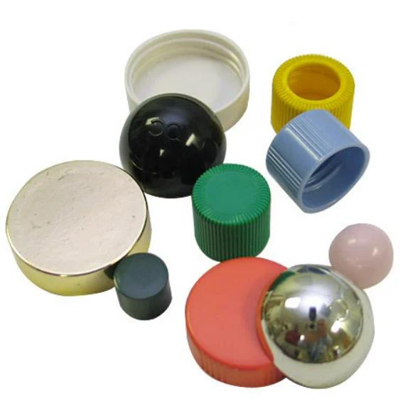
- Aesthetic appeal: PVD coatings create durable decorative finishes—gold (titanium nitride), black (chromium nitride), and bronze (zirconium nitride) for jewelry, watches, and automotive trim. They resist tarnishing and scratching.
- Dimensional accuracy: Coatings as thin as 10 nm preserve tight tolerances (±0.001 mm), critical for precision parts like semiconductor wafers and medical instruments.
- Adhesion: Ion bombardment during deposition creates strong bonds (10-50 N/cm² in pull tests), preventing peeling even under thermal or mechanical stress—essential for aerospace components.
- Thermal resistance: Ceramic coatings (hafnium carbide) withstand temperatures up to 3000°C, protecting rocket nozzles and turbine blades in extreme environments.
Applications of Vacuum Deposition
Vacuum deposition enables innovation across high-tech industries:
- Semiconductors: CVD deposits ultra-thin (1-100 nm) dielectric and conductive films (silicon dioxide, copper) on wafers, forming the layers of integrated circuits. ALD ensures atomic-level precision for 5 nm and smaller chips.
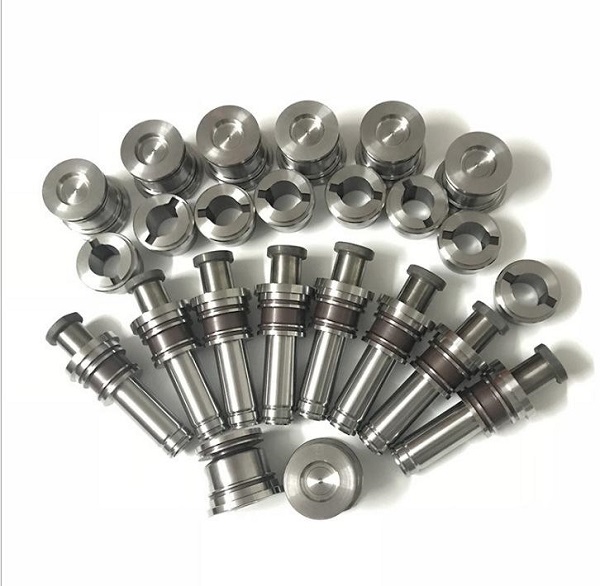
- Cutting tools: PVD coatings (titanium aluminum nitride, TiAlN) on drills, end mills, and inserts reduce friction and heat, allowing faster cutting speeds and extending tool life by 3-10x. They’re used in machining steel, titanium, and composites.
- Medical devices: DLC coatings on surgical tools reduce tissue adhesion, while PVD titanium coatings on implants (hip joints, stents) improve biocompatibility and prevent corrosion in the body.
- Optics: Evaporated coatings (magnesium fluoride, aluminum) on lenses and mirrors create anti-reflective, reflective, or filter properties. Telescope mirrors use aluminum evaporation for 90%+ reflectivity.
- Aerospace: CVD ceramic coatings protect turbine blades from high temperatures, while PVD chromium coatings on landing gear resist corrosion and wear in harsh environments.
- Consumer electronics: PVD coatings on smartphone frames (stainless steel, aluminum) add scratch resistance and premium finishes (black, gold). DLC on screens reduces glare and fingerprints.
- Jewelry: PVD gold and platinum coatings on stainless steel or titanium create affordable, durable alternatives to solid precious metals. They resist tarnishing and are hypoallergenic.
Vacuum Deposition Process and Equipment
The vacuum deposition process and equipment are engineered for precision and control:
- Vacuum chambers: Stainless steel or aluminum chambers (0.1-5 m³) with viewports and ports for pumps, sources, and gas lines. They’re sealed to maintain 10⁻³ to 10⁻⁹ Torr vacuum.
- Deposition sources:
- Sputtering targets: Solid disks (titanium, chromium) mounted in cathodes, bombarded by plasma ions.
- Evaporation sources: Crucibles (tungsten, alumina) for resistance heating, or electron beam guns for high-melting materials (tungsten, ceramics).
- CVD reactors: Inject gas precursors (silane, titanium tetrachloride) that react on the substrate surface.
- Pumping systems: Combine roughing pumps (rotary vane) to reach 10⁻³ Torr, then high-vacuum pumps (turbomolecular, ion) for 10⁻⁷ to 10⁻⁹ Torr.
- Gas supply systems: Deliver inert gases (argon for sputtering) or reactive gases (nitrogen, oxygen) to form compounds (TiN, Al₂O₃) at controlled flow rates (10-100 sccm).
- Substrate holders: Rotating fixtures (1-10 RPM) ensure uniform coating on complex shapes. Heaters (room temp to 1000°C) improve adhesion and crystallinity.
- Pre-treatment processes: Substrates are cleaned via plasma etching (removes contaminants) or ion bombardment (roughens surface for better adhesion), critical for coating quality.
- Quality control equipment: Ellipsometers measure film thickness (1 nm precision), scratch testers evaluate adhesion, and X-ray diffraction (XRD) analyzes crystal structure.
Quality Control and Maintenance in Vacuum Deposition
Rigorous quality control and maintenance ensure consistent, high-performance coatings:
- Thickness measurement: Ellipsometry and X-ray fluorescence (XRF) verify thickness (±1% of target), critical for semiconductors (where 1 nm variation affects device performance).
- Adhesion testing: The scratch test (ASTM C1624) uses a diamond stylus to measure the load at which coating fails—acceptance criteria vary by application (e.g., >30 N for cutting tools).
- Surface inspection: Optical microscopy (50-1000x) checks for pinholes, voids, or uneven coverage. For semiconductors, defect density must be <1 per cm².
- Equipment maintenance: Vacuum pumps are serviced monthly (oil changes, filter replacement) to maintain pressure. Targets are replaced when worn (after 50-100 runs) to ensure uniform deposition.
- Process parameters: Chamber pressure, gas flow, power, and substrate temperature are logged and controlled within ±2% of setpoints. SPC (Statistical Process Control) identifies drift before defects occur.
- Quality standards: Compliance with ISO 14644 (cleanroom standards) for semiconductors, ASTM F1580 (medical coatings), and ISO 18553 (PVD for tools) ensures reliability.
- Defect correction: Pinholes are reduced by improving vacuum or pre-treatment. Uneven thickness is fixed by adjusting substrate rotation or source power distribution.
Yigu Technology’s Perspective
As a leading custom manufacturing supplier in China, Yigu Technology offers advanced vacuum deposition services, including PVD (sputtering, evaporation) and CVD for automotive, medical, and electronics industries. Our systems achieve coating thicknesses from 50 nm to 5 μm with ±5% uniformity. We specialize in TiN (gold), CrN (silver), and DLC coatings, with strict quality checks via ellipsometry and scratch testing. Our processes meet ISO 9001 and medical ISO 13485 standards, ensuring biocompatibility and durability. We tailor coatings to client needs—from high-hardness tool coatings to decorative finishes—delivering precision and reliability at scale.
FAQs
- How thick can vacuum deposition coatings be?
Most range from 10 nm (semiconductor films) to 10 μm (industrial tool coatings). Thicker coatings (up to 50 μm) are possible but may crack under stress. ALD excels at ultra-thin, uniform films (<10 nm).
- Are vacuum-deposited coatings biocompatible?
Yes—titanium, zirconium, and DLC coatings are biocompatible, used in implants and surgical tools. They’re tested to ISO 10993 standards to ensure no adverse biological reactions.
- How long do vacuum-deposited coatings last?
In industrial tools, PVD coatings last 3-10x longer than uncoated tools. Decorative coatings on jewelry or electronics resist wear for 5+ years with normal use. In harsh environments (aerospace), ceramic CVD coatings last decades.