Manufacturers seeking a material that combines extreme strength, electrical conductivity, and corrosion resistance often hit a wall. Most high-strength alloys sacrifice conductivity, while conductive materials like pure copper lack the durability for demanding applications. This is where Metal Stamping C17200 (Beryllium Copper) becomes irreplaceable. As a copper-beryllium alloy, C17200 delivers a rare blend of tensile strength exceeding 1,200 MPa and electrical conductivity up to 45% IACS, making it ideal for critical components. However, stamping it requires specialized expertise to handle its unique heat treatment needs and avoid brittleness. In this guide, we’ll address these challenges, exploring C17200’s properties, processes, and applications to help you achieve consistent, high-quality results.
Material Properties of C17200 Beryllium Copper
C17200’s exceptional performance stems from its precise composition: 97.7–98.5% copper, 1.6–2.0% beryllium, and trace nickel. This creates a material with standout characteristics:
- High Strength: Tensile strength ranges from 690 MPa (annealed) to 1,240 MPa (heat-treated), outperforming most stainless steels while remaining formable.
- Excellent Conductivity: 25–45% IACS (International Annealed Copper Standard), balancing strength with electrical performance—critical for components like connectors and switches.
- Corrosion Resistance: Superior to most copper alloys, C17200 resists saltwater, industrial chemicals, and atmospheric tarnishing, making it suitable for marine and aerospace environments.
- Hardness: Heat-treated C17200 reaches 38–42 HRC, comparable to tool steel, ensuring wear resistance in moving parts like springs and contacts.
- Thermal Stability: Maintains properties at temperatures up to 200°C, preventing degradation in high-heat applications like engine sensors.
These properties make C17200 the material of choice for parts where failure is not an option.
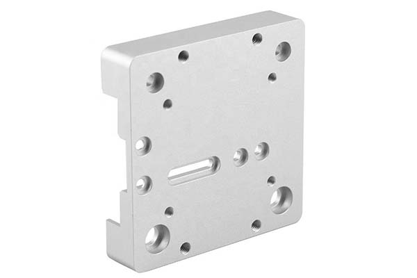
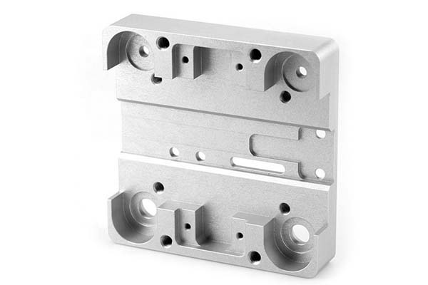
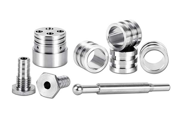
Manufacturing Process for Stamping C17200 Alloy
Stamping C17200 requires a strategic approach to leverage its heat-treatable nature:
- Stamping Process Stages: C17200 is typically stamped in its annealed state (soft temper) for maximum formability, then heat-treated to achieve full strength. This two-step process avoids cracking during forming.
- Die Design: Use carbide dies with polished surfaces (Ra ≤ 0.2 μm) to prevent galling, as C17200’s hardness can accelerate tool wear. Maintain punch-die clearance of 8–10% of material thickness to ensure clean edges.
- Blanking and Forming: Blanking requires high-pressure presses (300–500 tons) to handle annealed C17200’s toughness. For forming, use gradual bends with a minimum radius of 1× material thickness to avoid surface defects.
- Heat Treatment: After stamping, solution anneal at 780–820°C for 30 minutes, quench in water, then age at 315–330°C for 2–4 hours. This precipitates beryllium-copper compounds, increasing strength by 60–80%.
- Surface Finishing: Electroplating with gold or nickel enhances conductivity and corrosion resistance, critical for electrical contacts in harsh environments.
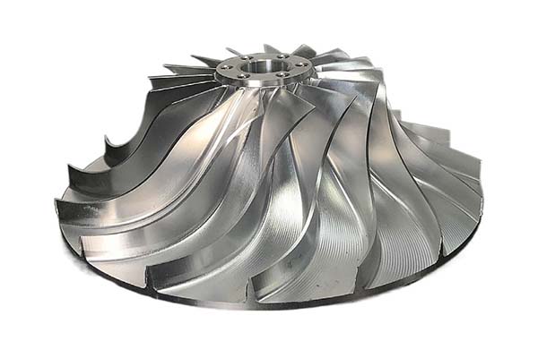
Applications of C17200 Beryllium Copper Components
C17200’s unique properties make it indispensable in high-performance industries:
- Electrical Connectors: Ensures reliable signal transmission in aerospace wiring and medical devices, where low resistance and durability are critical.
- Springs: Powers battery contacts and valve springs in automotive systems, withstanding millions of cycles without fatigue.
- Aerospace Parts: Used in landing gear sensors and avionics, where strength, conductivity, and corrosion resistance meet strict safety standards.
- Tooling: Forms precision molds for plastic injection, leveraging its high hardness and thermal conductivity for consistent part cooling.
- Electronic Devices: Found in smartphone antennas and computer connectors, balancing miniaturization with performance.
Each application relies on C17200’s ability to perform under extreme stress, temperature, and corrosion.
Quality and Standards for C17200 Beryllium Copper
Maintaining C17200’s performance requires adherence to strict standards:
- ASTM Standards: ASTM B194 specifies chemical composition and mechanical properties, ensuring C17200 meets tensile strength requirements (minimum 1,035 MPa after heat treatment).
- ISO Certification: ISO 13373 outlines testing procedures for beryllium copper, including conductivity measurements and hardness testing.
- Material Testing: Conduct tensile tests on heat-treated samples to verify strength, and use eddy current testing to confirm conductivity (≥25% IACS for electrical applications).
- Dimensional Accuracy: Use CMMs to maintain tolerances of ±0.005 mm for critical features like contact points, ensuring proper fit in assemblies.
- Surface Finish Specifications: Require Ra ≤ 0.4 μm to prevent electrical arcing in connectors and reduce wear in moving parts.
Yigu Technology’s Perspective
As a custom manufacturing supplier in China, Yigu Technology specializes in Metal Stamping C17200 (Beryllium Copper) for aerospace and medical clients. We control the entire process—from annealing to heat treatment—to ensure parts meet ASTM standards, with strict testing for strength and conductivity. Our expertise in die design and surface finishing ensures C17200 components deliver reliable performance in critical applications, balancing precision with the alloy’s unique material demands.
FAQs
- How does C17200 compare to phosphor bronze for springs?
C17200 offers 30–40% higher tensile strength and better conductivity but at 2–3× the cost. Use C17200 for high-stress, high-conductivity needs; phosphor bronze for cost-sensitive applications.
- Is beryllium copper safe to stamp?
Yes, with proper handling. Beryllium dust is toxic, so use ventilation systems and avoid dry grinding. Annealed C17200 (before heat treatment) is less brittle and generates less dust.
- What’s the maximum thickness for stamping C17200?
Practical for sheets up to 1.5 mm thick. Thicker material (1.5–3 mm) requires pre-annealing and slower press speeds to prevent cracking during forming.